There is one company every advanced chip will depend on for the next decade, and this week it collected commitments from every foundry that matters.
On September 7 and 8, TSMC and ASML announced a joint initiative to transition the chipmaking industry from its decades-old 6-inch photomask standard to a new 12-inch format, with major chipmakers committing to the direction around the SPIE/BACUS Photomask Technology conference in Monterey, California.
Now both TSMC and Samsung have committed to High-NA EUV roadmaps. Samsung says it plans to deploy High-NA EUV in mass production of DRAM by 2028, while TSMC has said it intends to use High-NA in high-volume manufacturing for advanced nodes starting in 2030.
Those are not vague expressions of interest. They are dated production commitments, on the record, from companies that move carefully before saying anything in public.
What Changed This Week
TSMC says it intends to use ASML’s High-NA technology in high-volume manufacturing for advanced nodes starting in 2030, and expects the number of layers requiring High-NA EUV to rise as device architectures get more complex.
Samsung committed to deploying High-NA EUV in mass production of DRAM by 2028. If it hits that target, it would mark the first time any chipmaker has used High-NA EUV in the DRAM sector.
The larger photomask initiative targets establishing a 12-inch mask pilot line by 2031, supporting full lithography system readiness for advanced-node production by 2033. The transition to larger 12-inch masks is expected to lift fab productivity, reduce chip manufacturing costs, and eliminate stitching limitations.
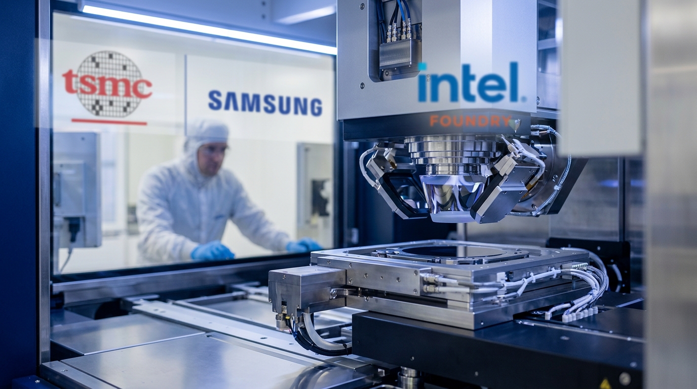
Intel is not waiting for 2028. High-NA is already being used in high-volume manufacturing at Intel Foundry, with more than one million wafers processed to date. That includes high-volume manufacturing on select layers for a subset of Core Ultra Series 3 processors, code-named Panther Lake.
Why the Business Case Is Exceptional
ASML is the only supplier of EUV lithography equipment globally. That is the entire thesis in one sentence. No competitor can build these machines. The physics, the optics supply chain centered on Zeiss, and a decade of process knowledge are not reproducible on any foreseeable timeline.
ASML’s High-NA EUV machines cost around $400 million each. With Samsung committing to DRAM production and TSMC to logic, the addressable market for High-NA systems expands well beyond Intel’s current volumes.
The financial momentum already reflects this. In its Q2 2026 results, ASML reported total net sales of €9.3 billion with gross margin of 54.0%, both above guidance. And on its Q2 2026 investor call, management said it is planning to add about 30% EUV capacity for 2027 versus 2026, and that it will also look into a 30% increase in capacity for 2028.
According to a widely followed S&P Global-compiled analyst consensus published on September 8, 2026, 43 analysts rate ASML a “Strong Buy,” with an average 12-month price target implying roughly 23% upside from then-current levels.
What Could Go Wrong
The risks are real. The upbeat outlook could be challenged if export controls tighten further on EUV tools or if geopolitical tension disrupts ASML’s China business and long-term demand expectations. ASML has said it expects China to represent about 20% of net sales in 2026, a concentration that carries obvious regulatory risk.
Valuation is the other honest concern. The stock’s trailing P/E has been cited around 60x in recent market-data summaries, and some valuation services characterize it as trading above their estimated fair value. A multiple that high leaves little room for execution slippage.
The 12-inch photomask initiative also carries execution risk. The industry still has to prove mask quality, defect inspection, handling reliability, overlay performance, and economics across the supply chain. A pilot line by 2031 is a target, not a guarantee.
The Bottom Line
Three foundries. One supplier. Dated commitments stretching into the early 2030s. That is not a speculative thesis, it is a confirmed demand signal backed by the companies that determine where global chip production goes next. The valuation asks investors to pay up, and the China exposure deserves genuine scrutiny. But ASML has rarely held a stronger hand than it does this week, and the companies placing their bets made that clear in Monterey.